IBM's sub-1 nanometer chip tech: potential AI hardware implications and what builders should monitor
Published by AINave Editorial • Reviewed by Ramit
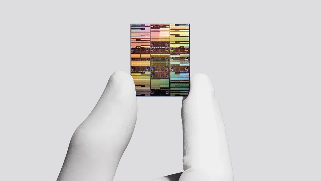
IBM has unveiled the world's first sub-1 nanometer chip technology, a research breakthrough that could reshape AI hardware design if it reaches commercial scale. The new nanostack architecture packs up to 100 billion transistors on a fingernail-sized die, nearly double the density of IBM's 2 nm node, and promises up to 50% higher performance or 70% greater energy efficiency. For AI builders, this means potential future accelerators with dramatically lower power consumption for inference and training, but the technology remains years from production.
What happened
IBM announced a sub-1 nanometer chip technology featuring a nanostack architecture that packs up to 100 billion transistors on a fingernail-sized die. The sub-1 nm node uses three nanosheets each 5 nanometers thick (about 15 atoms) with 9 nm sheet separation, and stacks are staggered across two separate wafers connected by a dielectric bond. Fast Company
IBM claims up to 50% higher performance or 70% greater energy efficiency versus its 2 nm node, plus a 40% improvement in SRAM, which is critical for AI inference. The architecture can be customized for CPUs, GPUs, and mobile chips. Fast Company
Commercial deployment is anticipated within five years. IBM is currently partnering with Japanese foundry Rapidus to scale 2 nm manufacturing, and all three major foundries (Intel, Samsung, TSMC) have initiated mass production of 2 nm chips based on IBM's earlier technology. IBM will announce manufacturing partners for the sub-nanometer chips at a later time. Fast Company
Why AI builders should care
If scalable, the new architecture could meaningfully boost AI inference workloads and cloud AI acceleration due to higher transistor density and energy efficiency. The 40% SRAM improvement directly benefits AI model execution where SRAM is a bottleneck. Fast Company
The architecture supports customization for CPUs, GPUs, and mobile chips, suggesting potential future heterogenous AI accelerators. Industry-wide impact depends on commercial adoption and manufacturing scale, given competition around 2 nm nodes from Intel, Samsung, and TSMC. Fast Company
Practical implications
The sub-1 nm NanoStack architecture could enable more powerful AI chips with similar or reduced power envelopes, benefiting AI inference and cloud workloads. SRAM gains (40%) could improve AI model running time in inference paths where SRAM is a bottleneck. Fast Company
Commercial deployment timing remains speculative and dependent on partnerships and manufacturing readiness. IBM projects five years, but sub-nanometer manufacturing at scale has not been demonstrated. Ars Technica
Caveats
IBM's claims are primarily based on a press release and third-party coverage; practical feasibility at production scale is unproven. Mass manufacturing of sub-nanometer nodes is not yet demonstrated, and partnerships for production are to be announced later. Ars Technica
Comparisons to 2 nm node performance and efficiency are projections and may not translate identically in real workloads. The node names now refer to generations of manufacturing technology rather than exact physical dimensions. Fast Company
FAQs
What is sub-1 nanometer chip technology?
IBM describes a sub-1 nm node as a manufacturing process and design rules beyond 2 nm, using atomic-scale engineering and a nanostack architecture. Key features include nanosheets about 15 atoms thick and a dielectric-bonded two-wafer stack. Read more on Fast Company.
How many transistors on IBM's sub-1nm chip and what could that mean for performance?
IBM claims up to 100 billion transistors on a fingernail-sized die, roughly double the density of its 2 nm node. Performance and efficiency gains are projections from IBM's technical results and have not been validated in production-scale workloads. Details on Fast Company.
What is the nanostack architecture and how does it enable this breakthrough?
Nanostack stacks transistors across two wafers with a novel dielectric bond, creating a denser, cross-wafer arrangement compared to traditional layer stacks. This enables the sub-1 nm density. Explanation on Fast Company.
When will IBM's sub-1nm chips be commercially deployed and who will manufacture them?
IBM aims for commercial deployment within five years. Manufacturing partners for the sub-nanometer chips have not yet been announced as of the update. Timeline on Fast Company.
Sources
- IBM debuts world's first sub-1 nanometer chip technology
- IBM Debuts World’s First Sub-1 Nanometer Chip Technology
- IBM claims world’s first sub-1 nanometer chip technology
- World-First Nanometer Chip Technology and the Future of...
- A New Frontier For Semiconductors As IBM Unveils The World’s First...
- IBM debuts new chip technology that could make your phone last...
- IBM just packed 100B transistors into a fingernail-sized sub-1nm chip — is it rewriting Moore's Law?
- IBM says new sub-nanometer architecture paves the way for the next decade of chip design
- IBM hails new 'block of flats' design breakthrough for ultra tiny chips
- IBM has unveiled chip technology that could help extend Moore’s Law another decade
- IBM shares jump after company says it's produced the first sub-nanometer microchip
- IBM debuts new chip technology that could make your phone last...
- Tech Xplore provides the latest news from IBM
- IBM says it has built the first sub-1nm chip technology
- IBM says it can fit nearly 100 billion transistors on a chip - why the milestone matters
- IBM Debuts World's First Sub-1 Nanometer Chip Technology